Author Topic: New to repairs; JDM-030 buttons are all mixed  (Read 1670 times)

Offline CaptainDapper

  • Guppy
  • *
  • Posts: 2
  • Post quality +0/-0
  • Acidmods User
New to repairs; JDM-030 buttons are all mixed
« on: April 28, 2020, 09:00:31 AM »
Almost everything on this board works just fine. Triangle, Square, and X when pressed all seem to press each other at the same time. I suspect there's a resistor that is broken somewhere, but I don't know where to begin. Nothing on the board sticks out to me, but I'm new to the lower-level fixes, so I don't know for sure. I guess I'll just a few questions and see where it goes from there.

Has anyone had this same issue before? Are there any diagrams for button lead resistors/caps for the 30? Could it be something else? The traces look fine, and the ribbon daughter board seems perfectly fine; none of the traces mix or break.

Offline RDC

  • Administrator
  • Around the block
  • *
  • Posts: 2608
  • Post quality +90/-2
  • Gender: Male
  • The CGnome Project
Re: New to repairs; JDM-030 buttons are all mixed
« Reply #1 on: April 28, 2020, 04:14:05 PM »
Haven't' seen that issue before, and each button line makes it's own way back to the MCU, so there's really nothing but the contacts and the daughter boards (the plastic flex circuits) then the rubber/silicone pad that sits under the buttons with their contact material.

I'd give everything a good cleaning first with a Q-tip and some rubbing alcohol. All the contacts on the daughter board, the contacts on the button pads, and look over the button pad good, make sure it's not cracked or really worn out. I can't see it being so weak that one button press causes the other 2 to drop far enough to register, but I've seen weirder things.
Screwing up is one of the best learning tools, so long as the only thing you're not learning is how to screw up.

Offline CaptainDapper

  • Guppy
  • *
  • Posts: 2
  • Post quality +0/-0
  • Acidmods User
Re: New to repairs; JDM-030 buttons are all mixed
« Reply #2 on: April 29, 2020, 08:47:50 PM »
So I've cleaned all the contacts. I'll have to try a new daughter board for it, but in the meantime I tested it out and I hadn't exactly remembered the issue. As it turns out, X and Triangle press each other, but that's it. Everything else works flawlessly.

If a new daughter board doesn't do it (which I don't see why it would; this one looks perfect, and X and triangle lines don't even go near each other), then I'm wondering if there is corrosion underneath the ARM chip. At least, I assume that's where the inputs end up.

Speaking of which, I'm a totes newb but there must be traces we can't see, since the contacts go to vias that are surrounded entirely by ground... How does that work, and is it possible to tell where those lines end up? Sorry if this is a stupid question, I really appreciate the help and information

Offline RDC

  • Administrator
  • Around the block
  • *
  • Posts: 2608
  • Post quality +90/-2
  • Gender: Male
  • The CGnome Project
Re: New to repairs; JDM-030 buttons are all mixed
« Reply #3 on: April 30, 2020, 09:57:46 AM »
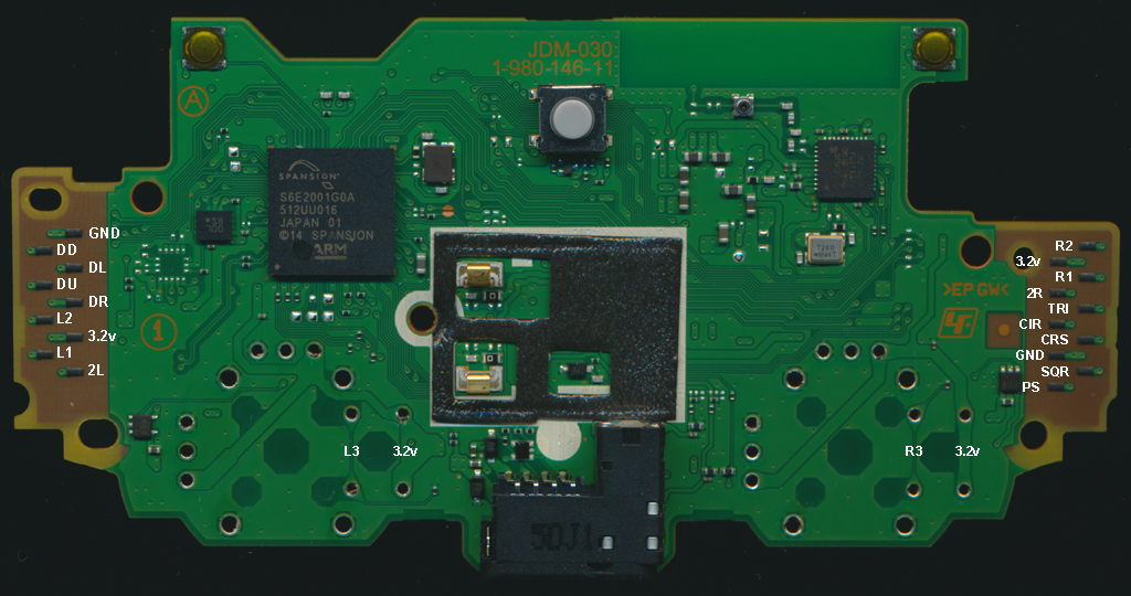
The PCB is multi-layer, at least 4 of them on that one, stacked in there like layers of a cake. Typically you'd have Top, Inner 1, Inner 2, then Bottom for a 4 layer board. When you see a via that goes from the Top or Bottom to nowhere on the other side, it's connecting something on the Top or Bottom to an inner layer. If you see a via that has no connection on either side, it's connecting something in the Inner layers together, aka Inner 1 to Inner 2.

There's only 3 ways to know for sure where the traces all run to, one of them will never happen and the other 2 destroy the board in the process.

1 - Get the schematic from Sony. Never going to happen.
2 - Strip the board of almost every component and spend countless, tedious hours probing around it with a meter to see what goes where. Not practical and the number of points you'd have to check would be beyond ridiculous for a human to do by hand, and even if you did manage to start that task, the board would be poked to death near the end of it and likely have some damage that caused false readings, to say nothing of the spots you would miss just being human.
3 - Strip the board of every single component and then scan the PCB, then remove the solder mask and scan it again, then the fun part, strip the top and bottom layers and then yep, scan it again. Then you can virtually trace every single spot from start to end. This also takes countless, tedious hours, but gets you an exact layout of the board, for that version of controller anyway. I did this with a JDM-055, don't recommend it, but it works.

Corrosion could do it, but I'd imagine there would be other signs of corrosion on the board as well as it causing several other issues, but again, weirder things have happened. The odds of something getting under the BGA and shorting those 2 lines together and nothing else are kind of astronomical.

Has this controller ever worked correctly? If that's an unknown, then it could be it's had the issue since it was made and there was an etching problem with that board and those lines are connected somewhere on/in the PCB. You can try checking the Resistance from X to /\ and see what it is, then check from X or /\ to other buttons and see if there are any glaring differences. If you prob onto the black contacts you'll get some Resistance from them, and you don't want to go stabbing those all up anyway, so try to prob just back form them on the actual trace.

Also try the same test on the Daughter board to make sure some short between the X and /\ isn't hiding in plain sight there.


Screwing up is one of the best learning tools, so long as the only thing you're not learning is how to screw up.


SMF spam blocked by CleanTalk
SimplePortal 2.3.5 © 2008-2012, SimplePortal